Understanding Semiconductor Parts in Modern Electronic Systems
Posted on December 22, 2025
griffin adams
Aerospace
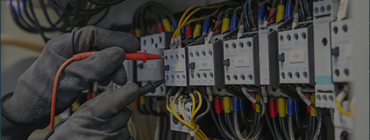
Semiconductors serve as critical components in many modern electronic systems, a result of their notable ability to regulate current flow, condition signal behavior, and maintain stable processing performance across a wide range of operating conditions. To support these capabilities, semiconductor manufacturers often rely on controlled fabrication procedures that establish specifically desirable electrical characteristics well before the component is installed within a circuit. In this blog, we will examine the common production processes, layout considerations, and handling protocols that can contribute to reliable semiconductor performance in demanding environments, so read on if you are interested in learning more.
What Manufacturing Processes Promote Semiconductor Part Quality and Consistency?
Effective semiconductor production regularly hinges on carrying out careful fabrication sequences that shape device characteristics accurately while minimizing the risk of contamination and structural variability. Generally speaking, common production processes include:
-
Photolithography Sequences: Manufacturers often use structured exposure and masking procedures to define specific circuit patterns across wafers, enabling consistent device geometry in the face of high-volume production.
-
Doping and Ion-Implantation Steps: The controlled introduction of a dopant is carried out during wafer fabrication to define specific carrier concentration levels and junction behavior, enabling finished semiconductor devices to achieve desired electrical performance characteristics.
-
Etching Processes: Wet and dry etching methods are commonly followed to remove semiconductor material in a controlled manner, forming device boundaries that support stable electrical behavior.
-
Wafer-Level Inspection: Automated metrology systems can be utilized to assess potential surface defects, verify pattern alignment, and evaluate junction integrity, allowing technicians to identify any deviations before production moves into subsequent phases.
-
Final Electrical Testing: Completed semiconductor devices may undergo electrical verification procedures to evaluate operating thresholds, leakage characteristics, and functional behavior before packaging.
How Do Semiconductor Switching Behaviors Affect Circuit Timing and Control?
The switching behavior of semiconductor devices plays a central role in determining how particular components will respond to control inputs, maintain timing relationships, and regulate energy flow across various circuit conditions.
-
Rise and Fall Time Characteristics: Transitional intervals during switching events influence edge definition and signal integrity, requiring engineers to align timing parameters with the performance specifications of subsequent circuit stages.
-
Switching Loss Considerations: The energy dissipated during transitions can impact conversion efficiency and thermal loading, making switching losses a critical factor to consider during thermal management design.
-
Gate-Drive Requirements: Insulated-gate devices commonly require accurately defined drive voltages and waveform profiles so they can transition between states in a consistent and controlled manner.
-
Propagation Behavior: Certain semiconductor topologies may introduce intrinsic propagation delays as control signals traverse internal structures, influencing phase alignment and timing coordination in cascaded circuitry.
-
Reverse-Recovery Profiles: Diodes and rectifiers undergo finite reverse-recovery intervals after conduction, which can affect efficiency in high-frequency applications that involve rapid commutation cycles.
How Do Semiconductor Layout Choices and PCB Interaction Affect Electrical Performance?
Beyond the aforementioned factors, semiconductor behavior is also strongly shaped by how each device interfaces with its supporting printed circuit board. This means that layout configuration will play a direct role in determining electrical performance across varied operating conditions.
-
Trace Routing Strategies: Semiconductor routing paths are often designed to maintain specified current density limits, helping associated circuit components maintain reliable electrical performance under varying load conditions.
-
Parasitic Element Control: Conductor spacing is routinely managed to reduce unintended inductive or capacitive coupling, allowing designers to minimize timing deviations in sensitive circuits.
-
Ground-Plane Utilization: Defined grounding architectures are regularly implemented to limit noise coupling and support stable semiconductor operation, benefiting applications where signal margins may be narrow.
-
Component Spacing Decisions: The physical separation of components will generally be specified to accommodate desirable thermal dissipation requirements, all while reducing the likelihood of unwanted electromagnetic interaction between adjacent devices.
-
EMI/EMC Management Techniques: Layout features that enhance electromagnetic compatibility are consistently incorporated for semiconductor devices to operate reliably in environments that are subject to elevated electrical interference.
What Storage and Handling Practices Help Maintain Longterm Semiconductor Quality?
Following manufacturing and assembly, semiconductor components need to be stored in controlled conditions and handled properly to support consistent electrical performance.
-
ESD-Safe Handling Protocols: Operators should always use grounded wrist straps, properly conductive work surfaces, and antistatic transport containers to limit the risk of electrostatic discharge events that could compromise junction integrity or latent device reliability.
-
Moisture-Sensitivity Precautions: Moisture-sensitive components should be stored in dry-pack materials or packaged with desiccants to limit moisture absorption that may lead to defects.
-
Temperature-Controlled Storage: Facilities will often maintain defined temperature ranges in storage spaces to reduce the likelihood of thermally induced material changes or degradation.
-
Shelf-Life Tracking and Labeling: Standardized labeling and date-based traceability systems bolster precise inventory management, ensuring semiconductor components can be used before time-dependent degradation risks increase.
Browse Our Selection of Semiconductor Parts at Your Convenience
There is no better purchasing platform than Industrial Universe for competitive options on new, used, obsolete, and hard-to-find diode components, bridge rectifier parts, and other semiconductor products that are sourced from a network of reputable manufacturers and suppliers. Unlike other purchasing platforms that might ask you to decide between reliability, pricing, and timely delivery, we strike an ideal balance for fulfillment with our leading services. If you are ready to experience all that we have to offer, get in touch with a member of our staff today and begin sourcing desired items from our expansive database.


 The only independent

 All Orders are Fulfilled in the U.S.A.